
Welcome back to earnings season! Over the next several weeks, I will be sending 40 detailed reviews on popular, high-quality companies. The Netflix article will be published later tonight, with ServiceNow, Tesla, Robinhood, Meta, SoFi, AMD, Palantir and so many others coming thereafter.
If you'd like access to all of those reports, consistently thorough weekly news, my real-time performance/portfolio updates and access to a large Discord channel of seasoned investors, lock in your annual deal below.
This is where investors (including Fortune 500 executives) come for signal over noise and to invest with good reason.
Other recent content includes:
a. Taiwan Semi 101
Taiwan Semi manufactures chipsets for designers like Nvidia, Amazon, AMD, Broadcom and Qualcomm. It does so in its highly expensive and complex chip fabrication plants. These are called “fabs” for short.
Needed Definitions:
- Fab means a factory.
- Nanometer (NM) describes the chip manufacturing technology. Smaller NM is more advanced, as it uses smaller transistors. This means TSM can pack more transistors into a single chip, making those chips more energy efficient and cost-effective.
- “Advanced Technology” revenue is revenue from 3-nanometer (N3), N5 & N7 technology. Anything under N7 is “advanced.”
- These labels describe the actual manufacturing technology process.
- Wafer refers to the raw materials (usually silicon) that are used to manufacture chips. Wafers are the “substrate” that integrated circuits (ICs) are built on top of. The transistors within these ICs guide and facilitate functions. Nvidia’s Blackwell chips are considered ICs.
- Lithography is the process of using photomasks (chip blueprints) and light to print chip patterns onto wafers. A light-sensitive material is added to wafers, with light pushed through the masks to guide the chip's design. This closely guides how light and chemicals generate desired patterns and create specific use cases. Lithography is paramount to TSM’s production."
- While traditional foundry services entail the actual testing and creation of a chip on a silicon wafer, packaging involves storing, integrating and prepping chip components with thermal protection, connectivity equipment and encapsulation (physical damage protection).
- These categories (packaging, testing and mask-making) are part of TSM’s “Foundry 2.0” – or the firm’s updated overall foundry total addressable market (TAM).
- Chip-on-wafer-on-substrate (CoWoS) is a packaging process that combines chips into a single unit. It allows things like GPUs, high-bandwidth memory (HBM) and custom chips to be vertically stacked and connected on a single substrate. This improves the compute speed and performance generated from these chips. TSM is a key partner for all HBM manufacturers. It doesn't actually build the memory layer of these memory chips, but does provide the infrastructure to layer on and package other needed components.
- Substrates also help protect chip components and manage heat.
- Vast processing needs from GenAI and Agentic AI require the vertical stacking CoWoS facilitates to ensure needed access to scalable data.
- AI Accelerators, as the name indicates, accelerate high-performance compute (HPC) workloads in the realm of AI. GPUs are a type of AI accelerator, along with Application Specific Integrated Circuits (ASICs) (custom chips) and Google’s Tensor Processing Units (TPUs; for machine learning). TSM also includes high-bandwidth memory in this category. HBM facilitates ultra-low latency, high-bandwidth support for querying and data processing tasks as a wonderful complement to GPUs, for example.
b. Key Points
- N2 is scaling on schedule.
- TSM needs more N3 capacity to meet demand.
- Supply conditions remain tight.
- Modestly raised CapEx guidance.
c. Demand
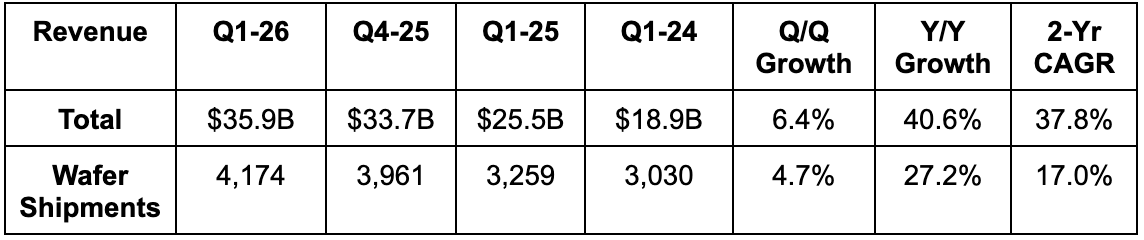
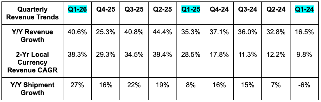
Taiwan Semi beat revenue estimates by 1.4% & beat guidance by 2%. Its 37.8% 2-year compounded annual growth rate (CAGR) (in U.S. dollars) compares to 21.1% last quarter and 38.4% two quarters ago. Advanced technology demand stemming from the explosion in AI agents again drove the strong growth this quarter.
Splits by Technology:
- N7 was 13% of revenue vs. 14% last quarter and 15% Y/Y.
- N5 was 36% of revenue vs. 35% last quarter and 36% Y/Y.
- N3 was 25% of revenue vs. 28% last quarter and 22% Y/Y.
- Advanced Tech was 74% of revenue vs. 77% last quarter and 73% Y/Y.
Splits by End Market:
- High-Performance Compute (HPC) revenue was 61% of total vs. 55% Q/Q & 59% Y/Y.
- HPC revenue rose by 20% Q/Q vs. 4% growth last quarter.
- Smartphone revenue was 26% of total vs. 32% Q/Q and 28% Y/Y.
- Smartphone revenue rose by -11% Q/Q vs. 11% growth last quarter.
- Internet of Things (IoT) revenue was 6% of total vs. 5% Q/Q & 5% Y/Y.
- Auto revenue was 4% of total vs. 5% Q/Q & 5% Y/Y.
d. Profits & Margins
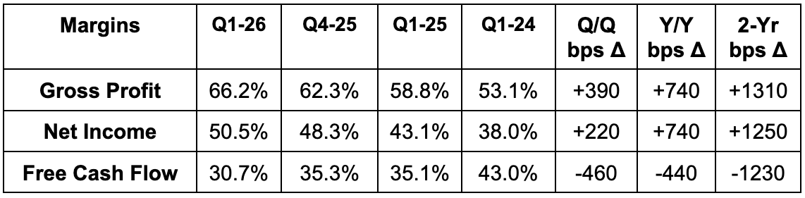
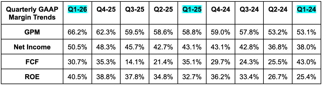
- Beat 64.3% GPM estimates by 190 bps & beat guidance by 220 basis points (bps; 1 basis point = 0.01%) . Much more on factors influencing this metric later in the piece.
- Beat EBIT estimates by 5.9% & beat guidance by 7.5%. Its 58.1% EBIT margin beat 57% margin guidance.
- Beat $0.66 EPS estimates by $0.04.
- EPS rose 58% Y/Y in local currency.
- Beat 38% return on equity (ROE) estimates.
e. Balance Sheet
- $105B cash & equivalents.
- Inventory +6% Y/Y.
- $31.6B bonds payable.
- ~0% Y/Y diluted share growth.
- Accounts Receivable Turnover was 26 days vs. 26 Q/Q and 28% Y/Y. Inventory Turnover was 80 days vs. 74 Q/Q but still lower than 83 days Y/Y.
f. Guidance & Valuation
Upgrade below to read through guidance, valuation, notes from the call and my take on the quarter that I think will surprise many.